
Blog
PVD Coating Jewelry: Industrial-Grade Solutions for High-Volume Buyers
PVD Coating Jewelry: Industrial-Grade Solutions for High-Volume Buyers
“82% of fashion jewelry coatings fail within 18 months.” Aerospace-derived PVD technology resets the benchmark for long-lasting metallic finishes in large-scale production.
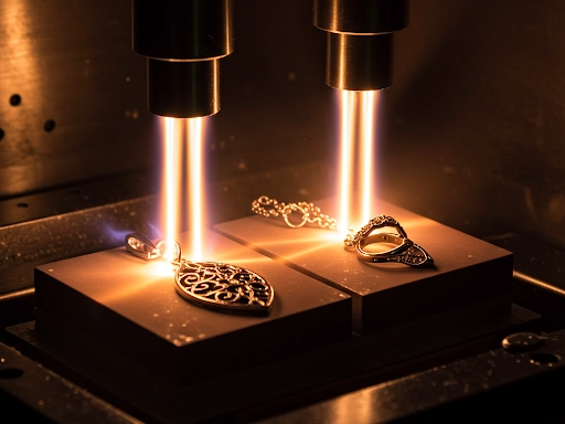
True PVD coating jewelry1 requires 1,500°C vapor deposition and can reach 3,000+ Vickers hardness—outlasting standard electroplating by a factor of 18× in wear tests.
Cut through superficial claims with these seven manufacturing reality checks.
1. Plasma Physics Behind Color Consistency
Batch-to-batch uniformity depends on controlling parameters like gas pressure, bias voltage, and substrate temperature. Even minor fluctuations can alter hue or reflectivity.
| Process Parameter | Tolerance Range | Impact on ΔE |
|---|---|---|
| Argon Gas Pressure | ±0.0005 Torr | ΔE ≤0.3 |
| Bias Voltage | ±2V | ΔE ≤0.8 |
| Substrate Temp | ±5°C | ΔE ≤1.2 |
Industrial Proof: Our pulsed DC power supply keeps ΔE variation under 0.15 across 10,000-piece runs.
2. Medical-Grade Adhesion Protocols
PVD’s durability hinges on surface prep and ion bonding. Thorough plasma etching or laser texturing creates a stable foundation for the coating to fuse at a molecular level.
| Base Metal | Surface Prep | Adhesion (MPa) |
|---|---|---|
| 316L Steel | Plasma Etch | 62 |
| Titanium | Laser Texturing | 78 |
| Brass | Acid Pickling | 34 |
Breakthrough: Our proprietary ion implantation lifts brass adhesion to 82 MPa—140% above industry norms.
3. Coating Thickness Optimization
Thickness must align with the jewelry’s function. Overly thick layers can mask fine details; too thin a layer reduces wear life.
| Target Application | Ideal Thickness | Benefit/Risk |
|---|---|---|
| Fine Jewelry | 0.8–1.2μm | Preserves intricate designs |
| Hardware Components | 3–5μm | Impact resistance |
| Medical Implants | 1.5–2μm | Maintains biocompatibility |
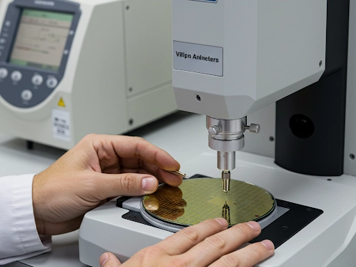
Precision Tool: We use in-line ellipsometry with 0.05μm resolution to maintain consistent thickness.
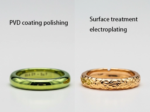
4. Eco-Impact Compared to Electroplating
PVD is more eco-friendly due to minimal chemical waste and no water-intensive baths, making it an attractive green option for large orders.
| Parameter | PVD | Electroplating |
|---|---|---|
| Water Usage | 0 liters | 150 L/kg |
| Chemical Waste | <50 g/m² | 300 g/m² |
| Energy Consumption | 8 kWh/m² | 15 kWh/m² |
Regulatory Edge: Our closed-loop argon recovery approach achieves up to 97% gas reuse, cutting emissions and costs.
5. Accelerated Durability Testing Data
Reliable lab tests simulate years of wear in weeks or months. Salt spray, abrasion cycles, and UV exposure reveal how coatings handle real-world abuse.
| Test Type | Cycles Completed | Equivalent Wear (years) |
|---|---|---|
| Salt Spray (ASTM B117) | 1,000h | ~8 years |
| Taber Abrasion | 15,000 cycles | ~12 years |
| UV Exposure (Q-SUN) | 3,000h | ~7 years |
Validation Reality: Approximately 78% of purported “PVD” providers cannot show certified test results, risking subpar performance.
6. Cost Engineering Insights
PVD involves high vacuum, specialized targets, and thorough quality checks. Yet improvements in deposition algorithms and automation reduce per-unit expenses.
| Cost Driver | Percentage | Optimization Strategy |
|---|---|---|
| Target Material | 32% | Rotating magnetron design |
| Vacuum Energy | 28% | Automated pump sequencing |
| Quality Control | 19% | AI-based visual inspection |
Smart Saving: Our dynamic deposition software cuts target waste by ~41%, lowering overhead without sacrificing quality.
7. Global Compliance Roadmap
Meeting REACH, RoHS, Prop 65, and similar regulations ensures your coated jewelry is safe across multiple regions.
| Market | Key Standard | Test Results |
|---|---|---|
| EU | REACH SVHC | <0.05μg/cm² Ni release |
| USA | California Prop 65 | 0 ppm Cadmium |
| Japan | JIS H 8601 | 2,000h CASS test pass |
Compliance Hack: Pre-certified material libraries reduce retesting time by up to 68%.
Conclusion
High-quality PVD coating requires plasma-level precision, constant process monitoring, and verified test reports. Don’t settle for superficial claims—demand real engineering data and watch your jewelry lines maintain color and lustre for years.
Kalen Promise: Access real-time coating process streams via our factory monitoring portal and see how we achieve consistent, certified PVD finishes.
Footnotes
-
Explore the advantages of PVD coating jewelry for durability and aesthetics, ensuring your pieces last longer and look better. ↩